Image Gallery
Gallery
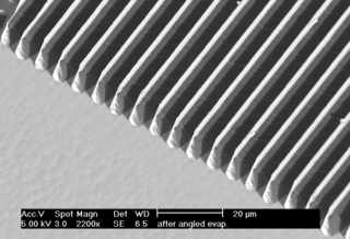
Anisotropic Etching of a Bulk Silicon Wafer
Media Details
Created 1/18/2005
ESEM image of smooth sidewalls of single crystal silicon formed by anisotropic wet etching. The underlying Si was chemically etched anisotropically using KOH/H 2 O solution.
Credits
- John A. Rogers , 3D Micro- and Nanosystems, Beckman Institute
- Jong-Hyun Ahn , 3D Micro- and Nanosystems, Beckman Institute